Deconstructing the Layers of Advanced PCBs:A Comprehensive Guide
Introduction to PCB Layer Architecture
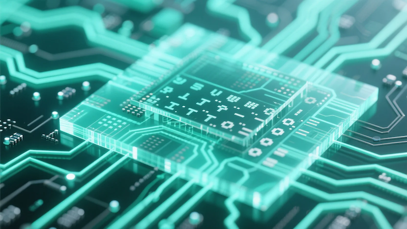
The printed circuit board (PCB) serves as the backbone of every modern electronic device, and understanding its layered composition is fundamental to grasping its functionality. Each layer is meticulously designed to perform specific roles, from signal transmission to mechanical support and electromagnetic protection. Omini, a leading EMS provider, understands that the intricacies of PCB manufacturing and PCBA assembly necessitate a thorough knowledge of these layers. This guide offers an in-depth exploration of the critical components that form the foundation of PCB manufacturing, highlighting the technologies and processes involved, particularly in SMT assembly and rigid-flex solutions.
Understanding the Copper Layers: The Foundation of Connectivity
The most fundamental PCB layers are the copper layers, which provide both electrical connectivity and structural support. Omini leverages advanced manufacturing techniques to create precise copper pathways that facilitate reliable signal transmission across PCB assembly projects. These conductive layers define the pads necessary for surface-mount and through-hole components, with the latter featuring plating structures to ensure proper connections.
The importance of copper layers is self-evident – they serve as the primary current pathways in the printed circuit board layout. Standard copper thickness typically ranges between 1 and 3 ounces per square inch (oz), with industry standards varying from 0.0005 inches to 0.003 inches or thicker. PCB manufacturing involves exacting processes to maintain these specifications, ensuring consistent electrical performance. For prototype PCB development, careful consideration of copper layer counts is crucial for balancing functionality with cost-effiveness.
Copper Pour Techniques: Functionality and Optimization
PCB assembly includes two distinct approaches to copper distribution: large-area copper pour and grid-style pattering. The former creates broad, continuous copper areas optimally suited for distributing electrical power while providing electromagnetic shielding benefits in SMT assembly applications. Although this approach offers advantages, particularly in thermal management and electromagnetic compatibility (EMC) performance, it requires careful engineering to prevent issues like wave soldering blistering.
Grid copper pours represent another critical implementation within PCB manufacturing, offering excellent heat dissipation characteristics while maintaining precise control over signal routing and impedance matching. These grid structures play a vital role in EMS provider-level projects requiring stringent electromagnetic compatibility, effectively acting as both thermal management systems and electromagnetic barriers. The strategic implementation of these copper distribution methods significantly enhances the overall reliability of both rigid-flex and conventional PCB designs.
The Role of Substrate Layers
The substrate layer forms the mechanical backbone of any printed circuit board, supporting and insulating the conductive layers while providing structural integrity. This foundational layer, commonly constructed from FR-4 material in standard PCB manufacturing, plays a crucial role in determining board flexibility required for applications involving rigid-flex PCB technology or space-constrained designs. Other specialized materials like Teflon (PTFE) or polyimide may be chosen based on specific project requirements – each offering distinct advantages in thermal management or electrical insulation properties versus FR-4’s cost-effectiveness and availability.
Omini engineering teams expertly select substrate materials according to application specifications, understanding that the substrate choice impacts signal integrity, thermal conductivity, and overall PCB assembly quality. This attention to detail ensures optimal performance in complex electronic systems ranging from consumer devices to industrial equipment, meeting the rigorous demands of today’s electronics market.
Solder Mask Layers: Protection and Precision
The solder mask layer serves as critical protection for the underlying copper features, defining the areas where solder paste can be applied during PCB assembly operations. This polymeric coating prevents solder bridges between adjacent conductors while offering environmental protection against moisture, contaminants, and thermal stress. Precision PCB manufacturing processes ensure uniform application of solder mask layers, maintaining consistent thickness specifications throughout the production run.
An essential aspect of EMS provider service at Omini involves optimizing these mask layers according to design rules that prevent manufacturing defects. The design parameters govern opening sizes, annular rings, and mask thickness to ensure reliable assembly outcomes. By establishing stringent quality controls around solder mask application, Omini ensures consistent manufacturing results while maintaining signal integrity requirements necessary in complex circuitry.
Silkscreen Layers: Information and Instructions
The silkscreen layer represents more than just visual elements; it serves as the informational backbone for component placement and board identification. Standard alphanumeric information includes reference designators (footnotes), component polarity indicators, and specific pin identification (especially for integrated circuits). These elements must be properly spaced from electrical features to avoid manufacturing complications during PCBA assembly.
Omini places importance on clear silkscreen implementation, recognizing that proper reference designators directly translate to efficient assembly processes and maintainability throughout a product’s lifecycle. The strategic placement and formatting of silkscreen information minimize production errors and streamline final testing verification, factors that contribute significantly to time-to-market for turnkey PCBA services.
Copper Pad Layers: Interface Foundations
These specialized PCB layers establish the interface points between components and the board’s conductive pathways. Precise control over pad size, shape, and surface finish enables reliable component attachment and electrical connection in both surface-mount and through-hole PCB assembly techniques. Omini employs advanced plating processes, including nickel-gold, silver, or tin finishes, to enhance solderability while preventing oxidation of exposed copper surfaces.
Strategic Implementation in PCBA Services
The comprehensive consideration of each PCB layer configuration allows Omini to consistently deliver high-performance printed circuit boards across diverse applications. By understanding how the interplay between copper distribution, substrate selection, masking parameters, and informational layers affects overall board performance, the team at Omini optimizes each EMS provider relationship through tailored turnkey PCBA services that meet unique project requirements.
Understanding these intricate details not only illuminates the manufacturing process but highlights the expertise required for advanced PCB manufacturing and complex SMT assembly operations. These insights represent the foundational knowledge necessary for designing and implementing sophisticated electronic systems that meet the demanding requirements of modern technology.